The Critical Cost of Routing Congestion
by On Jul 17, 2014
The Growing Expense of Wires in SoC Design May Be Costing You Critical Design Wins
It’s impossible not to notice – SoC designs are becoming more complex. Markets require greater performance, smaller die size, more functionality and lower cost without sacrificing power efficiency. As if this never-ending hunger for complexity weren’t enough, SoCs are increasingly constrained by the growing number of wires required to make connections to the different functional portions and IP blocks within the design.
Design teams are often plagued with increased wire count that can produce routing congestion. The drawbacks are so significant that they often negate cost, performance, power efficiency and reliability advantages. Companies lose opportunities for critical design wins in high-volume or emerging-growth markets when their SoCs can’t compete in these crucial areas.
The place and route (P&R) stage of chip design is critical for abating wire congestion. Designers are seeking ways to avoid the following symptoms:
- Increased die size
- More metal mask layers
- Higher defect rate
- Longer wire routes
- Greater number of unpredictable critical paths
- Longer time to market
- Higher costs
- Greater power consumption
- Increased latency
The challenges stem from reliance on in-house interconnect fabrics for linking the growing numbers of IP blocks on the SoC. With each generation of chipmaking process technology, standard cell sizes shrink. So do wire widths, but not as much. As a result, the silicon area lost to wire routing congestion is increasing. This trend contributes to larger, more spread-out floor plans that decrease the amount of dies each wafer can yield and increase the amount of defects per die. A more spread-out floor plan also makes wire routes longer, which reduces the predictability of critical paths.
One way to decrease floor-plan size is to add more metal layers to the fab process. However, an increase in layers and masks adds to manufacturing expense and also increases defect rates.
Benefits of Packetization and Serialization
Top semiconductor design teams are addressing congestion by adopting Network on Chip (NoC) technology for the interconnect. As opposed to using standard bus transaction interfaces to send traffic between increasing numbers of IP blocks, design teams are discovering that NoC technology provides the benefit of serialization and packetization in SoC designs.
Serialization and packetization can cut the number of wires in half. They also reduce the size of the buses connecting IP and maximize the utilization of each wire.
- Packetization takes the SoC transaction data and places them on the same wires as address, control and command signals. This results in far fewer wires to move data around on the chip compared with using standard socket or transaction interfaces.
- With serialization, the data can be transmitted on even narrower channels, thus shrinking wire count on chips. Designers can also trade wires for throughput and transaction latency to gain a greater degree of freedom compared with standard interconnect designs.
Consider this example: A minimal configuration of a 64-bit AXI interface requires 272 wires. A 64-bit packet-based channel within an Arteris NoC delivers nearly the same bandwidth with just 157 wires. Furthermore, the channels within an Arteris NoC can adapt serialization with no additional latency to provide more or less bandwidth as required by the application.
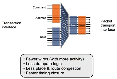
Having fewer wires means that a SoC can be designed with less data-path logic. The NoC approach allows designers to make data paths narrower and reduce wire counts to alleviate congestion.
Bottom line: A NoC requires far fewer wires and less logic to move data between IP blocks than older interconnect technologies like buses and crossbars.
In the end, the NoC approach provides:
- Accelerated time to market
- Smaller die size
- Optimized floor plan
- Lower cost
- Higher performance
- 50 percent reduction in total wire length
- Reduced power consumption
Adopting an Arteris NoC reduces complexity for the SoC design and enables faster time to market. Design teams are achieving better results in their efforts to shrink die size, boost performance, reduce cost and improve power efficiency. These advantages are creating the industry’s most competitive products.
Arteris goes into greater depth about the advantages of a packet-based NoC approach and provides more detail on the benefits of serialization in a white paper entitled Routing Congestion: The Growing Cost of Wires.
By Jonah Probell, Senior Solutions Architect, Arteris.
Mr. Probell has held development and support roles in the semiconductor IP business for 14 years and can be reached at jonah@arteris.com