INUITIVE CASE STUDY
Innovative NoC Implementation Dramatically Speeds Derivative Design
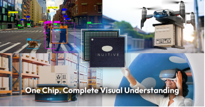
Founded in 2012, Inuitive is a fabless semiconductor company that designs and develops powerful multi-core processor integrated circuits (ICs) that serve as the vision processors for a wide range of smart devices. These application areas include robotics, drones, AR, VR, AIoT, and depth-sensing applications, that need complete visual perception.
Inuitive’s Vision-on-Chip processors are setting a new standard by introducing all-in-one chips with a wide range of integrated capabilities, outstanding performance, and optimal size and cost efficiency. These processors support simultaneous depth sensing, enhanced AI performance and VSLAM capabilities, while dramatically shortening both system latency and response time, saving power, and improving overall performance.
Inuitive’s vision-on-chip (VoC) devices employ advanced artificial intelligence (AI) combined with 3D imaging, computer vision and deep learning capabilities to make smart devices, products, and systems faster and smarter. These all-in-one chips offer extended multi-core vision processing, enhanced high-quality depth sensing, AI-based object detection and recognition, and state-of-the-art simultaneous localization and mapping (SLAM) implemented in high-performance hardware rather than software.
The Inuitive team consists of multi-disciplined, experienced veterans. Their goal is to embed their technology in consumer electronics, focusing on robotic devices to improve the way machines see and understand the world around them.
Business Challenge
- Create a new iteration of an existing vision-on-chip device quickly and easily, meeting an aggressively short time-to-market schedule
Design Challenges
- Replace an existing function with a new one without changing the physical layout of the surrounding logic.
- Connect the new function with its larger number of AXI ports to the existing logic with its smaller number of AXI ports
Arteris Solution
- FlexNoC® interconnect IP
Results
- Saved a significant amount of time and effort for the internal Inuitive team, allowing them to focus on other critical areas.
- Gained the ability to profile the data passing through the NoC, thereby allowing Inuitive to verify performance goals were achieved.
- Presented the new device to the market months earlier than possible with an internally developed solution.
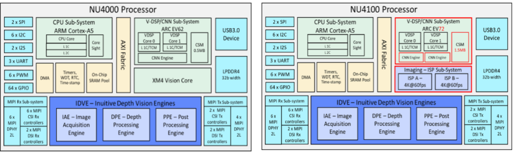
The Inuitive team faced a significant challenge when developing a derivative design based on the NU4000, their first vision-on-chip processor. The NU4000 is optimized for applications requiring a sophisticated combination of computer vision (CV) and 3D depth perception. It is equipped with three powerful CPU cores, three vector cores, a CNN engine, a depth processing engine, a SLAM engine and an advanced time warp engine. It can operate independently or be embedded as a co-processor for image processing and computer vision application.
The processor is optimized for mobile applications and markets, including VR head-mount displays, AR glasses, tablets, laptops and advanced robotics applications. The NU4000 is equipped with complete reference design modules that demonstrate how to best utilize the features of the device in various use cases and scenarios.
To meet the demands of cutting-edge customers, the Inuitive team introduced the NU4100, which can be viewed as a derivative design of the NU4000. The NU4100 replaced one of the NU4000’s three vector cores with a high-quality dual image signal processor (ISP) that supports 2x4K at 60 fps. The designers aimed to bring the NU4100 to market in record time. To achieve this goal, they needed to maintain the existing logic and physical layout to the greatest extent feasible.
The NU4000 employs the Advanced eXtensible Interface (AXI) on-chip communication bus protocol developed by Arm. However, removing one of the NU4000’s three vector cores resulted in access to only a limited number of AXI ports. The problem was that the new dual ISP required a greater number of AXI ports than were available. The challenge was to determine a way to connect the dual ISP with its larger number of AXI ports to the existing logic with its smaller number of AXI ports without changing the physical design of the existing logic. This was crucial to the success of the new design and time-to-market target since iterating the physical design is one of the most time-consuming phases when developing a silicon chip.
As Dor Zepeniuk, Co-founder and CTO at Inuitive said: “after exploring several alternatives, our ultimate solution involved employing a novel deployment of a network-on-chip (NoC) in the form of FlexNoC from Arteris.”
A typical system-on-chip (SoC) device involves a large number of intellectual property (IP) blocks, each implementing a complex function. Some of these functional IP blocks are designed in-house, while others are acquired from third-party vendors. Each functional IP block may employ one of the multiple interface protocols that have been defined and adopted by the SoC industry such as OCP, APB, AHB, AXI, STBus and DTL.
A NoC may be viewed as a special form of IP that spans the entire chip. Special interface functions called sockets are used to interface the functional IP blocks to the NoC. Some IP blocks act as initiators, generating data, others act as targets, receiving data, while some adopt both roles at different times. The socket associated with an initiator IP translates its protocol into a common packetized and serialized form, which is transported throughout the NoC. Multiple packets can be “in flight” at the same time. When a packet arrives at its destination, the socket associated with the target translates it back into the preferred protocol.
The Inuitive team realized that Arteris FlexNoC IP could be employed to create a special interface function to connect the new IP block, with its larger number of AXI ports, to the existing logic which has a smaller number of AXI ports. In this case, all the AXI ports on both the new IP and the existing logic are provided with their own sockets which are then connected to the special FlexNoC interface. Any data generated by an initiator is packetized, serialized, and conveyed to its target. As with a regular NoC implementation, each socket can have different properties such as width and frequency, and multiple packets can be transmitted simultaneously.
The ramp-up process to learn and deploy FlexNoC was fast and easy due to the excellent support we received from the team at Arteris.
Dor Zepeniuk
Co-founder and CTO, Inuitive

The result of using FlexNoC to implement the special interface function required by the NU4100 was a resounding success. As Dor says, “The ramp-up process to learn and deploy FlexNoC was fast and easy due to the excellent support we received from the team at Arteris.”
Using FlexNoC instead of designing a custom solution from the ground up saved the team a significant amount of time and effort. Furthermore, the FlexNoC IP enabled the team to profile the data passing through the NoC, thereby allowing them to verify that their performance goals were being achieved. Dor notes, “Using FlexNoC allowed us to get the NU4100 to market months earlier than if we had created a solution in-house.”
With respect to future plans, the Inuitive team has already commenced work on their next-generation vision-on-chip device. In this case, they have decided to employ FlexNoC as the primary interconnect IP for the entire chip. “That was one decision we didn’t have to think twice about,” says Dor.
Using FlexNoC allowed us to get the NU4100 to market many months earlier than if we had created a solution in-house.
Dor Zepeniuk
Co-founder and CTO, Inuitive