Busses, Crossbars and NoCs: The 3 Eras of SoC Interconnect History
by On Oct 22, 2010
The pat answer of course is “Moore’s law enabled semiconductor designers to cram more transistors into a given area each year, allowing more functions to be added to a chip.”
True.
But what is more interesting is the history of the critical part of the system that ties together all these functional IP blocks. I’m talking about the history of the interconnect.

The history of the interconnect has three phases. The first phase was driven by busses, with the first de-facto commercial standard being ARM’s Advanced Microcontroller Bus Architecture (AMBA). Originally released in 1996, AMBA consisted of two busses: An Advanced System Bus (ASB) for general SoC IP interconnect and an Advanced Peripheral Bus (APB) for slower peripherals. ARM followed these with the introduction of the Advanced High-performance Bus (AHB) to replace the ASB. However, many companies continued to own and developer their own bus interconnect IP.
As systems-on-chip grew in numbers of IP blocks, these busses began to show their limitations. Shared busses resulted in contention and hierarchal bus designs created complexity. There had to be a better way. And there was.
In 2003, ARM launched AMBA 3 which included the Advanced eXtensible Interface (AXI) while in 2001 the Open Core Protocol (OCP-IP) organization started work on what became the OCP specification. In both cases, these standards separated the interface from the interconnect topology, which was an improvement over traditional busses.
However the laws of unforeseen circumstances quickly intervened.
The physical implementation of these SoC interconnects required large, complex crossbars and integration with older bus-based IP required bridging and hierarchal designs. The interconnect became a gating factor at the physical place-and-route and floorplanning stages of SoC design, because the huge crossbars and numbers of wires could no longer be squeezed into the nooks and crannies between IP blocks as before. Furthermore, power consumption grew, SoCs did not meet their design frequencies due to timing closure issues, and many were delivered late because of multiple last-minute iterations between the place and route and RTL design teams.
The answer to these SoC floorplanning problems was clear: We needed to reduce the number of wires.
Packetizing data would allow it to be sent over smaller numbers of wires while having some type of guarantee of quality of service (QoS) for each transmission. Furthermore, distributing the interconnect logic throughout the chip rather than having massive chokepoint crossbars and switches would further simplify floorplanning.
An innovative company used these principles to create the world’s first commercial SoC network-on-chip interconnect.
More on this third era of SoC interconnect history next time.
Stay tuned…
Sources:
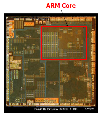
Apple A4 system-on-chip (SoC) photo courtesy of UBM TechInsights
