Connected by Arteris: Watching The Next Big Semiconductor Transition Unfold
by On Feb 14, 2024
Impressions from the 2nd Annual Chiplet Summit
From February 6th to 8th, 2024, a fascinating mix of engineers descended on the Santa Clara convention center for the Chiplet Summit. It felt like representatives from all aspects of the semiconductor ecosystem attended – providers of Semiconductor Intellectual Property (IP) like us, Electronic Design Automation (EDA) tool vendors, Wafer Fab Equipment (WFE) providers, Semiconductor Foundries, “Fabless” chip companies, and Integrated Design Manufacturers (IDMs) all in one place to discuss one thing – chiplets. The agenda varied from sessions discussing how to develop them, the architectures to integrate them, the substrates to assemble them on, the standards needed to connect them, the business models to enable them, and the industries and application domains setting requirements for them.
A bifurcated development landscape
The big takeaway was the not-so-subtle bifurcation of the development landscape, even though some of the panel discussions sometimes mixed and confused them.
On the one hand, chiplets are a reality and necessity today. Plenty of examples on the slides last week illustrated the designs of companies like AMD, Intel, NVIDIA, Apple, Google, Samsung, Meditek, Qualcomm, and HiSilicon. The main driver here is complexity. What developers used to integrate into one System-on-Chip (SoC) has reached the “reticle limits.” The complexity requirements exceed what fits onto one reticle, and yields decline when getting too close to the technology limits. I heard several references to a cost analysis that AMD did in 2021. The article “The Economics of Chiplets” offers an excellent summary. The key here is that the chiplets are essentially co-designed (with the exception, perhaps, of memory), and the companies mentioned above can control all design aspects, including, for instance, the Serdes technology at the chiplet boundaries, etc. It’s expensive to do that, and only a few markets offer the appropriate ROIs, and a few companies can afford the development NRE cost.
On the other hand – for everybody else who cannot afford to control all design aspects because they pay for them, there was a lot of discussion about an open ecosystem of chiplets. Instead of building an SoC with licensed IP blocks and added differentiation, can the design be integrated using reused chiplets? Are chiplets the next level of Semiconductor IP? An extreme example would be an SoC that was integrated monolithically in the past and is now wholly disaggregated into chiplets. One panelist called it, very fittingly, the “Legolization” of semiconductor design using chiplets. For this to work, many things need to fall in place. The industry needs to agree on standards for the PHY implementation between chiplets – UCIe, BoW, and XSR are in the running. The industry needs to agree on protocols for data transport between chiplets, considering networks-on-chips (NoCs). Amba AXI and CHI were very visible as candidates, and CXL also came up often. Most importantly, the industry must find business models and value propositions for chiplet-based designs outside the mega-big developments only a few companies can afford. That’s because the value mentioned above for massive designs (the AMD case) changes towards an IP-reuse type value in an “Open Chiplet Ecosystem” world.
We are looking at two fundamentally different paths here, with some technology overlap. Once established, UCIe or BoW-type standard interfaces can be helpful for both closed and open ecosystems.
Are we watching the next big transition in semiconductor design?
When it comes to EDA and development methodologies, if we think it through, chiplet-based can indeed be the next step. Abstractions have fascinated me throughout my career, and the predecessors of the graph below date back to the very early 2000s.
Alberto Sangiovanni Vincentelli’s The Art and Science of Integrated System Design (2002) had an early progression of the abstraction levels. In Selling System-Level Design (2012) I argued for an extension to transaction-level models for hardware/software development. Later, in The Next Level Of Abstraction For System Design (2015), I gave up on a proper executable specification driving everything from one definition. By the end of the decade, I was asking, “Does System Design Still Need Abstraction? (2019),” only to consider Multicore designs with their hardware/software environment the next level in Chasing The Next Level Of Productivity (2022).
The next step from here clearly seems to lead towards chiplet-based design – raising the entry-level from IP-based developments around platform-based design and multicore processors to chiplet-based design.
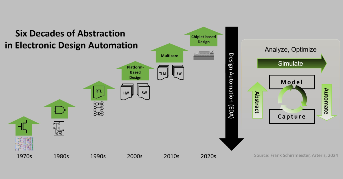
The industry is already implementing the classic path of abstraction, simulation at a higher level, and automation of implementation, as indicated on the right side of the graph above. Several vendors already showed high-level optimization using models of chiplets and their interfaces, like UCIe. Some even link down into the world of chiplet assembly considerations already.
Another phase of searching for more productivity begins!
How does Arteris fit in?
Our NoCs play a critical role in the data transport on and between the individual chiplets that users connect. Much discussion today revolves around the physical interfaces, but users also deal with complex protocol stacks on top of the physical connections between chiplets.
I participated on a panel, “Selecting the Right Interface for Your Applications,” organized by Palo Alto Electron’s CTO, James Wong, and moderated by Samsung Semiconductor’s David McIntyre. My co-panelists were Synopsys’s Mick Posner, Blue Cheetah Analog Design’s Elad Alon, Eliyan’s Kevin Donnelly, and Alphawave Semi’s Letizia Giuliano.
This panel is worthy of its own future Blog, and its themes revolved around the technical and practical aspects of chiplet technology, die-to-die interface specifications, their applications, performance metrics, scalability challenges, and the role of advanced simulation, testing, as well as AI/ML in optimizing design and adoption. We also discussed tradeoffs and application suitability of current and emerging die-to-die communication standards like UCIe and BoW and the impact of HBM and Photonics. We also touched on adoption challenges for die-to-die interfaces across various industries, the critical performance parameters for evaluating these technologies, and the difficulties in scaling.
In another session, My colleague Guillaume Boillet presented on “Efficient Data Transport in Chiplet-Based AI/ML Applications,” discussing the application of chiplet technology in AI/ML and the evolving landscape of chiplet-based designs for scalability, cost reduction, ecosystem development, and portfolio diversification.
Key drivers for adopting chiplets include scalability to address systems beyond critical limits, cost reduction through an emerging ecosystem and improved yields, ecosystem development for interoperability standards, and portfolio expansion. Guillaume emphasized the significant potential in enterprise computing, communication, and automotive sectors, with different values of chiplets across these verticals.
In the AI/ML context, Guillaume illustrated the need for scalable systems to support everything from cloud AI training to inferencing, highlighting the automotive industry’s interest in ADAS applications as a particular area of opportunity. He covered the technical aspects of chiplet design, including the preference for Mesh topologies and configurations for both coherent and non-coherent systems.
Guillaume detailed our strategy for partnering with PHY vendors and focusing on coherent and non-coherent interconnect solutions to meet the specific requirements of AI/ML applications and accelerators, emphasizing the importance of CXL port compatibility for chiplet-based AI accelerators.
You can find Guillaume’s and my presentation and a transcript here.
So, are we watching the next big semiconductor transition unfold?
Maybe. To me – very likely.
The chart I inserted above nicely shows the inevitability of abstractions in design methodologies as we, as end consumers, have this insatiable desire for more and more complex electronics, resulting in more and more electronics complexity.
What is unclear is the timeline. For the big companies that can control everything in their designs, chiplets are a reality today. The outlook toward an “Open Chiplet Economy” that represents the next level of abstraction for semiconductor design is probably much further out. Let’s check in where we are five years from now. The drivers to get there are very, very strong.